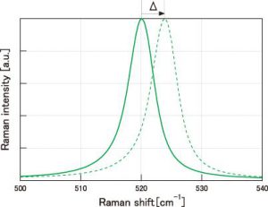
Exceeds 0.1cm-1 high accuracy peak shift analysis
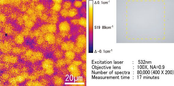
The images above show the distribution of grain boundary in a crystalline silicon thin film with optical microscope and Raman peak shift analysis respectively. Though the thin films seem to be crystallized uniformly with optical microscope, evidence of polysilicon-crystal grain boundaries can be observed by using the peak shift analysis that images the shift amount of Raman peak position of silicon.
About the sample used for measurement
This crystalline silicon thin film is produced by annealing 50nm thick amorphous silicon thin film used as a material of the thin-film transistor by Pulsed RTA method. Crystals are grown by using polycrystal in the thin film as a nucleus, and the thin film is crystallized uniformly.
*This sample was provided by Professor Yukiharu Uraoka of Nara Institute of Science and Technology.
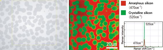
Observation of the distribution of amorphous and crystalline silicon (before annealing)
The two images below show the sample observation before annealing. The distribution of crystalline silicon and amorphous silicon in the thin film can be observed with either optical microscope or Raman image before annealing. In Raman image, green color and red color are assigned to show Raman peak of 520cm-1 come from crystalline silicon and broad peak of 470cm-1 come from amorphous silicon respectively.
(Reference)About peak-shift imaging
Small amounts of crystal strain can be detected by the shift amount of Raman peak position of the material. The obtained Raman spectrum is fit by the sum of two or more Gauss functions or Lorentz functions and this fitting parameter is made to an imaging. In RAMAN-11, the amount of the peak shift can be detected by high accuracy that exceeds 0.1cm-1.