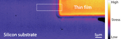
Raman Imaging of Stress Distribution on Silicon substrate
| Laser wavelength | 532nm |
| Obj. lens | 100x N.A.=0.9 |
| Grating | 2400 gr/mm |
| Number of spectra | 60,000(400×150) |
| Measurement time | 20 min |
The top image shows the distribution of peak shift of Si substrate. Raman imaging is a powerful tool to analyze the spatial distribution of stress around the boundary of thin film on Si substrate by quantifying the Raman peak shift.
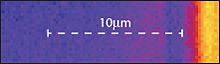
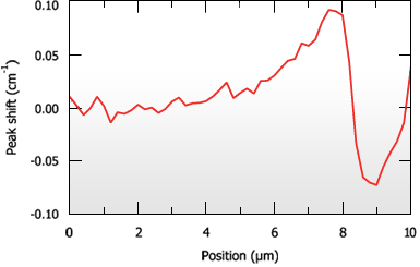
The right figure shows the shift of Si peak along the dot line. RAMANtouch can determine peak position more precisely than 0.1cm -1.
(Supplement)Spectral resolution and the precision of peak determination
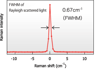
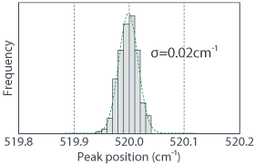
Spectral resolution is frequently misunderstood. “Spectral resolution” is fundamentally defined as the ability to separate close peaks. “Spectral resolution” depends on various factors such as focal distance of spectrometer, grating, and width of excitation laser. One can directly characterize the spectral resolution of a Raman microscope by measuring the width of Reilygh light. On the other hand, measurement of stress requires the precision of peak determination, which can be evaluated by the deviation of the peak positions of repeated measurements.