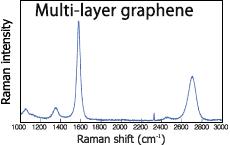


CVD method is expected as promising technique to product a large area graphene. The above figure shows a Raman image of graphene on epitaxial grown Ni thin film formed by CVD method. The image shows that single layer graphene was formed only in the Ni grain aggregate, and multilayer graphene was formed along the boundary of bicrystal. The multilayer graphene was formed by the segregation of carbon, and the bicrystal formation in the Ni thin film prevents the graphene from growing uniformly.
Courtesy of Advanced Technology Research Laboratories, Panasonic Co., Ltd.
Reference: S. Yoshii, K. Nozawa, K. Toyoda, et al., Nano Lett. 11 (2011) 2628-2633.