Materials applications/ed pressure or stress have internal strain in its crystal structure. The strain modulates frequency of Raman scattering light that is related with crystal structure and molecular oscillation of the materials. This is a feature of Raman scattering that is inelastic scattring with respect to Rayleigh scattering, which is elastic scattring of laser light with same frequency as Rayleigh light. The Raman spectroscopy is employed for stress-strain study, and the Raman imaging technique makes it possible to get a stress-strain image.
■Raman spectroscopy is a powerful tool for strain-stress study
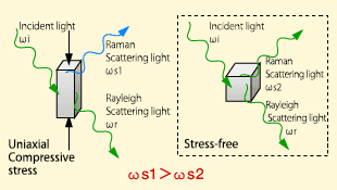
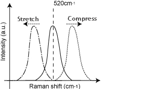
In a crystal with internal strain, Raman scattering light has a frequency shift compared with unstrained crystal. As shown in a figure below, Raman scattering light of silicon applications/ed compressive stress, expressed as Ws1, is shifted to high-frequency side compared with Raman scattering light of unstrained silicon, expressed as Ws2. Silicon has a optic mode, T2g mode, at 520 cm-1. The peak of 520cm-1 is sensitive to crystalline strain, and it is known that tensile (compressive) stain makes it shifted to low-frequency (high-frequency )side.

■Calculation of stain by the amount of peak shift
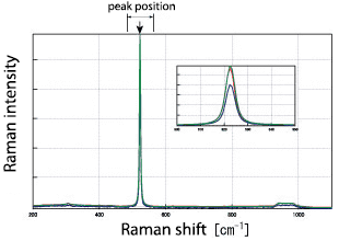
The amount of 520cm-1 peak shift is linearly increased with the amount of strain. Then, by measureing the amount of wavenumber shift precisely, we can know the accurate amount of strain. For the accurate measurements of the amount of wavenumber shift, a spectrometer with high spectrum resolution is needed. By making the dispersion of grating in spectrometer large, we can prepare it. We can determine the peak position by analyzing the spectrum data acquired by the spectrometer with peak fitting. Then we can evaluate the strain in the area of laser illumination by calculating the amount of the peak shift between experimentally detemined peak position and the peak position of unstrained silicon.

■Strain imaging of silicon
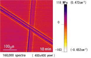
Defects and strain in the silicon crystal can be detected by Raman imaging. The right figure shows an image of scratch on silicon substrate. The Raman peak at the 520cm-1 is shifted by strain induced by applying stress into crystal lattice. By constracting the amount of the peak shift into an image, we can observe the strain distribution. Yellow part shows the shift into low-frequency side, and deep blue part shows the shift into high-frequency side. In the image, it is clearly observed that the crystal lattice is strained by compressive and tensile stress around the scratch. RAMANtouch can detect and image the peak shift of the order of 0.1cm-1.
RAMANtouch is available for Raman imaging of the strained silicon and thin silicon film. The acquisition time of the image is ultra fast, so that measurement can be done in a short time.
Measurement time: 10 min.
Stress = -250 MPa × Δν(cm-1)

