Email Magazine
Challenging Employees (11/25/2020)
Since its establishment in 2003, Nanophoton has continued to take on the challenge of developing new products and has released one after another products that no other company has. The company’s research and development staff is responsible for development. In this issue, we interviewed Koudai Saito, a senior researcher who joined the company in 2018, about the development of new products and how he joined the company. (e-mail Newsletter editor-in-chief / freelance writer Takeshi Nemoto)
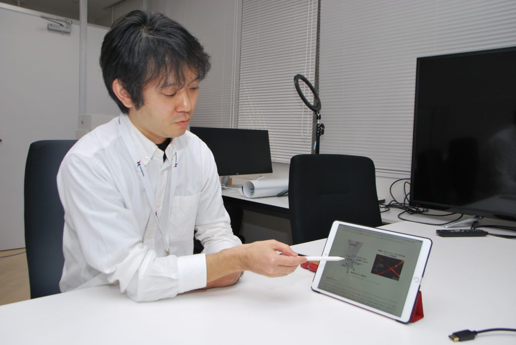
Nemoto: The Raman microscope is a device that measures the weak Raman scattered light emitted from molecules in a sample and shows the distribution of the molecules in an image. Up to now, we have introduced a number of new products, such as RAMANtouch, which is equipped with a new technology called line illumination and enables high-speed measurement, and TERSense, which realizes a high spatial resolution that exceeds the diffraction limit of light. What new products will be announced next?
Saito: I can’t go into details, but I have an idea and I’m in the process of preparing an experiment to verify the principle to see if it can be materialized.
Nemoto: I look forward to hearing about the success of the development. Have you been involved in research and development ever since you joined the company two and a half years ago?
Saito: No, from about six months after I joined the company, I also helped with manufacturing. I thought, “That’s not the same thing,” since I was now doing a lot of manufacturing, but I always liked making things, and it was a good learning experience for development. If you don’t know what’s inside a product, you can’t develop it. When I was actually assembling the RAMANtouch in the manufacturing operation, I felt that it was amazing that they were able to put the technology of line lighting into such a compact device. There are a lot of ingenious ideas in this product, and I think it will be difficult for other companies to imitate it.
Nemoto: You are a graduate of Keio University, but did you come into contact with Raman microscopes at that time?
Saito: I didn’t do optics to begin with. I went to university to study physics in the Faculty of Science and Engineering, and joined the condensed matter physics laboratory from my fourth year as an undergraduate until I received my doctorate in 2011. Within condensed matter physics, there is a field called low-temperature physics, which studies the properties of materials by cooling them to near absolute zero. In this laboratory, I developed an atomic force microscope (AFM) that operates in a low-temperature environment. I used it to measure the nanoscale friction on the surface of a superconductor in an attempt to measure some new physics.
Nemoto: What is an atomic force microscope?
Saito: It is a device that measures the shape of a sample by placing a nano-sized sharp needle close to the surface of the sample and measuring the atomic force acting between the needle and the sample. AFMs that work at room temperature are available on the market, but AFMs that work in cryogenic environments are hard to find. So, I made one myself.
Nemoto: How did you come across the Raman microscope?
Saito: When I was a graduate student, I wondered what kind of research I could do with AFM in the future. AFM is excellent for measuring the shape of nano-sized samples, but I thought it would be interesting to measure other information as well. At that time, I had a chance to hear about surface-enhanced Raman scattering (SERS) in a presentation by a classmate from another department; SERS is a phenomenon in which the Raman scattered light of a molecule is enhanced when the molecule is attached to a substrate with a bumpy surface made of gold or other particles. At the time, I had no idea about Raman or the enhancement effect of metals. I was very impressed, or rather, inspired.
At that time, I intuitively thought that it would be interesting to do this with the tip of an AFM needle. That’s exactly what tip-enhanced Raman scattering (TERS) is, but I didn’t know that it had already been invented at that time. After graduate school, when I was doing post-doctoral research on superconductivity, I searched for new things to do with AFM and light using keywords such as “AFM,” “Raman,” and “SERS,” and I was surprised to find TERS.
After some research, I found out that this kind of technology already existed. Further research revealed that it was apparently invented by a man named Satoshi Kawada. He seems to be at Osaka University. After that, I started looking at the homepage of Kawada Lab at Osaka University while surfing the Internet. Because it was outside my field, I never thought that I would later become a postdoctoral researcher at Kawada Lab and join Nanophoton, which was founded by Dr. Kawada.
Nemoto: So why the Kawata Lab?
Saito: My postdoctoral position was at the National Institute of Advanced Industrial Science and Technology (AIST, Tsukuba, Ibaraki), and at the end of my four-year project, there happened to be an opening for a postdoctoral position in the TERS project at Kawada Lab. The requirements were very narrow: the applicant had to have experience in building AFMs or STMs by themselves, and be familiar with electronic circuits and vacuum technology. I thought, “This is a great opportunity,” so I applied, and thankfully, I was hired. I joined the project in 2015.
Nemoto: Is that how you came to be a nanophoton?
Saito: The project at that time was to create TERS in the deep ultraviolet in collaboration with Nanophoton. Some of the results of the project have been commercialized as RAMANtouch vioLa, an ultraviolet and deep-ultraviolet laser scanning Raman microscope, and sumilé, a broadband reflective objective lens. After working with the members of Nanophoton, I realized that they have very high technology, and I wanted to work at Nanophoton to improve my skills. I wanted to work at Nanophoton to improve my skills.
Nemoto: You took a break from the development of equipment at AIST, but you have returned to the development of equipment.
Saito: Since I came to Kawata Lab as a postdoc, I have been developing devices again. I prefer to make things. It’s fun to be able to do that kind of work.
Nemoto: What do you want to do in the future?
Saito: Nanophoton’s TERS is a transmission type with high resolution and high sensitivity, but I have always wanted to make a reflection type TERS because I want to deal with samples on opaque substrates. However, I have always wanted to make a reflective TERS because I want to deal with samples on opaque substrates. In addition to this, I would like to create new products with my own ideas.