Email Magazine
Challenging Employees (5/26/2021)
When I first met Mariko Adachi, a senior engineer in charge of Sales & Applications at Nanophoton, she said, “I know the appeal of Nanophoton’s products. I was very impressed when she said, “I am full of love for equipment more than anyone else. The experience of encountering Nanophoton products and seeing them from the customer’s point of view during her previous job has been utilized in her current work. In this issue, we asked Ms. Adachi to share her “love” with us. (e-mail Newsletter editor-in-chief / freelance writer Takeshi Nemoto)
— What does Sales & Applications do?
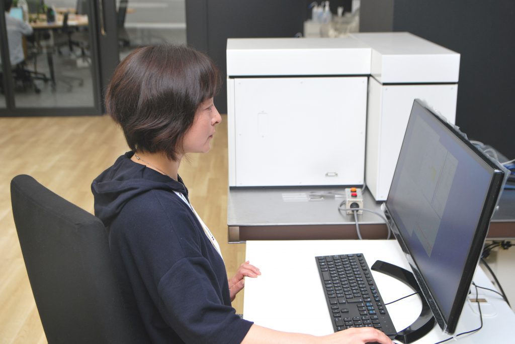
My job is to show how Raman microscope can be used in various fields. I actually measure customer’s samples and show them that “Raman microscope is effective in this way. I also hold lectures and seminars to explain the results. I also investigate how Raman microscopy can be used in fields that will be developed in the future, such as next-generation materials and power semiconductors.
— What does Sales & Applications do?Ms. Adachi once told me about her strong love for Nanophoton products. How did you come across Nanophoton’s Raman microscope?
After graduating from university, I joined a major semiconductor manufacturer and was involved in the evaluation of semiconductors at their Kansai office. When making semiconductors, evaluation is necessary for quality control and process monitoring. In the development and prototyping department of the front-end process of creating nanometer-level circuits on wafers (single crystals of semiconductors cut into thin sheets), I was in charge of inspection technology to determine what analysis techniques, timing, and frequency should be used to efficiently control foreign substances on wafers and defects that occur in the process. I was in charge of inspection technology. After that, I was transferred to a department that performs total evaluation and analysis of all processes and products. That was when I first learned about Raman spectroscopy, around 2010.
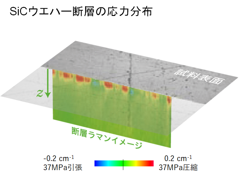
There is a technology to improve the performance of semiconductors by applying moderate stress to them. We used to use Raman spectroscopy to measure values for process development, such as how much force would make a good product and how much force would make a bad one. At that time, it was not a nanophoton product, but a Raman device to obtain a spectrum of a single point.
However, even if I told the people involved in the project with numbers and spectra, they wouldn’t understand it at all. I wondered what I should do, so I thought of imaging so that anyone could see it. But I had to move the stage little by little and measure each point one by one, which took about a month. I wanted a new device, so I went around to Raman manufacturers. That’s when I learned about nanophotons.
When I heard that it was a venture from Osaka University, I didn’t have high expectations until I went to see the demonstration. But they took the imaging data I had spent a month on in 20 minutes. “I was like, “I’m sorry, Nanophoton. When I came back to the company and showed the imaging data to the people concerned, they said, “Let’s improve it this way. When I returned to the office and showed the imaging data to the people concerned, they said, “Let’s improve it this way.” I realized that imaging data is necessary to move various people, and I realized the greatness of Nanophoton’s equipment.
—After that, you changed your job to Nanophoton?
Yes. The company was reorganizing its bases and the office I was working at was going to be closed. I was torn between transferring to the Kanto region or moving to a semiconductor manufacturer in the Tokai region, and at one point I decided to transfer to that manufacturer.
However, I thought I would change jobs after presenting my work that I had done for many years at an academic conference, so I was asked to wait for the final interview. Then, while I was having a break-up party with my colleagues at work, I received a phone call from my boss at the time saying, “Nanophoton is looking for an application engineer, so you should apply. I immediately applied and was hired in 2014.
I wouldn’t be here now if it weren’t for the fact that I had to delay my career change to present at a conference and that my boss found a job opening at that time. I think it was fate.
—How was your impression at the company?
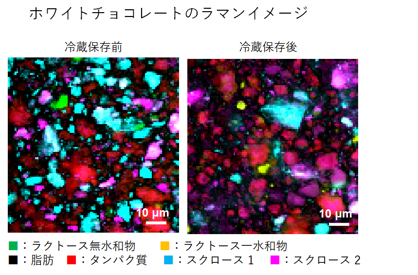
It was a series of surprises. To show that Raman microscopy can be applied to many different fields, we measured many different things. When I tried to measure white chocolate in the summer, I didn’t want it to melt, so I put it in the refrigerator and left the office, but when I took it out of the refrigerator the next day and measured it, I found that the distribution and spectrum of the material had changed due to moisture.
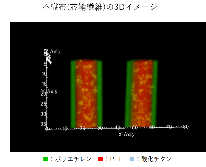
When I measured the core-sheath fibers of nonwoven fabrics, I was impressed by the 3D measurement results of the Raman microscope, as I had never thought before that there could be different materials on the outside and inside of a single fiber. Until then, Raman to me had only been a means of measuring stress, so this was the first time I learned that it could be used for various analyses in various fields such as lithium-ion batteries, pharmaceuticals, biotechnology, and nanocarbons.
Up until then, I had been working for a large company where tens of thousands of people were involved in the production of a single product, but at Nanophoton, I was impressed to see how such an amazing device could be made by so few people.
I’m also very open-minded. From my previous experience, I once proposed to make a Raman microscope for ultraviolet laser. I mustered up the courage to attend the development meeting, showed the materials, and appealed that “the future is the era of ultraviolet light. A few days later, Mr. Satoshi Kawata, Chairman of the Board of Directors, said, “I think we should make a Raman microscope with ultraviolet light. Then the development of the ultraviolet Raman microscope began. I was watching the development next to him, and I could tell that it was very difficult, but even so, as a “user representative,” I kept telling him about improvements and requests. In this way, the Raman microscope equipped with an ultraviolet laser was completed and sold. RAMANtouch vioLa, an ultraviolet/deep ultraviolet laser scanning Raman microscope with line illumination for high-speed measurement, was also developed. I was really impressed when I got the first data.
—I heard that you also requested the development of the RAMANdrive, a Raman microscope with wafer stage.
Yes. There was a customer who wanted to move to specific coordinates on a large wafer to see foreign matter, and we worked with them to commercialize the product.
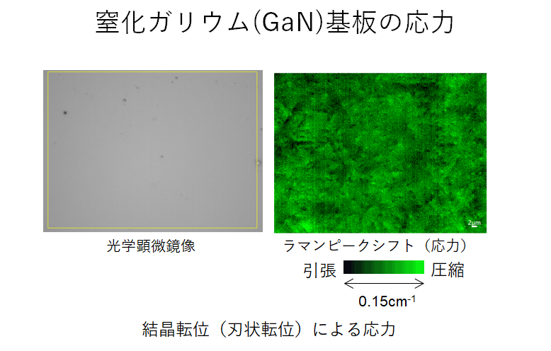
After that, I exhibited the completed RAMANdrive at a conference, and I felt that people in the semiconductor industry did not know about Raman as much as I thought. I felt that people in the semiconductor industry didn’t know Raman as well as I thought they would. Many of them didn’t know that they could easily see stress. Even if they knew about Raman, they still had the old image that it was difficult and time-consuming to measure.
Then I started to promote Raman. I wanted to tell people that Raman could accurately measure invisible stress distributions, and that the ability to accurately measure stress distributions could be used for any analysis other than stress. I held luncheon seminars, and when I was asked to write or give a lecture, I didn’t turn down any offer. In any case, I worked very hard to get Raman recognized.
—In addition to applications, you are also in charge of sales.
At first I was not sure how it would turn out, but it was surprisingly fun. I think the point of working with applications and sales is to be able to make technical proposals on how best to do things within a budget. Another good thing about working together is when the product is delivered. The customer is really looking forward to it. “There was even one person who said, “I woke up at four in the morning because I was so excited to see the device. There was even a time when a sample was waiting next to me while I was setting up the device.
It makes me very happy when people look forward to our equipment and are pleased with it. I think that our role is not to get customers to install our equipment, but to help them improve their products by collecting data with our equipment. We would like you to leave the Raman-related matters to Nanophoton and spend your time on research, commercialization, problem solving, and so on. That’s why we will make the device less fragile and easier to use.
I consider delivery as the beginning, not the end, and I try to receive phone calls and e-mails whenever there is a problem. “We also receive a lot of consultations from clients asking if we can do something like this, so we make proposals that meet their needs, and if new development is needed, we consult with our in-house development staff.
Nanophoton’s equipment has many new functions that were created based on customer requests, which I find very rewarding. I will continue to serve as a bridge to the development staff, so please keep sending us your requests, even if they are not possible with the current equipment.