Email Magazine
RAMANdrive (6/9/2021)
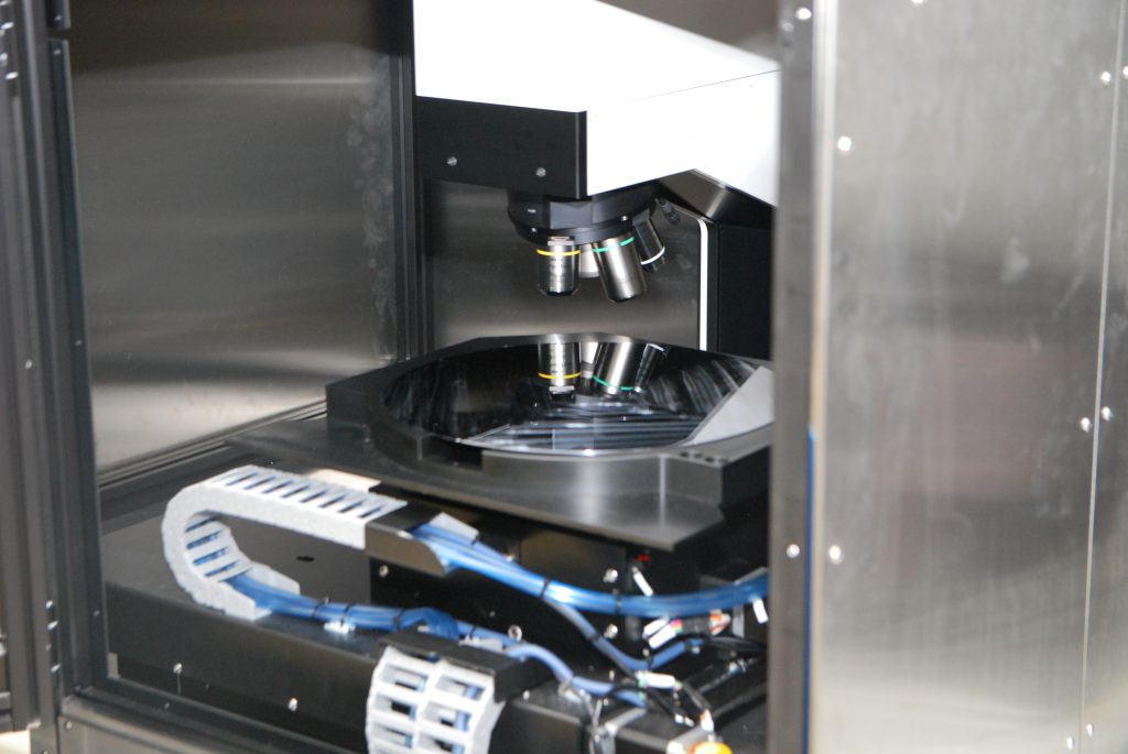
Last time, I interviewed Ms. Mariko Adachi, Senior Engineer in charge of Sales & Applications at Nanophoton. At that time, I also mentioned the development of RAMANdrive, a Raman microscope equipped with a wafer stage, but I regretted that I could not delve into it much. The RAMANdrive is amazing in that it can obtain Raman images of the entire surface of a wafer up to 30cm in size on a stage at a very high speed. The secret of this speed is a feature called AreaFlash. …… As in the previous article, Ms. Adachi told us about it. (Email Newsletter editor-in-chief / freelance writer Takeshi Nemoto)
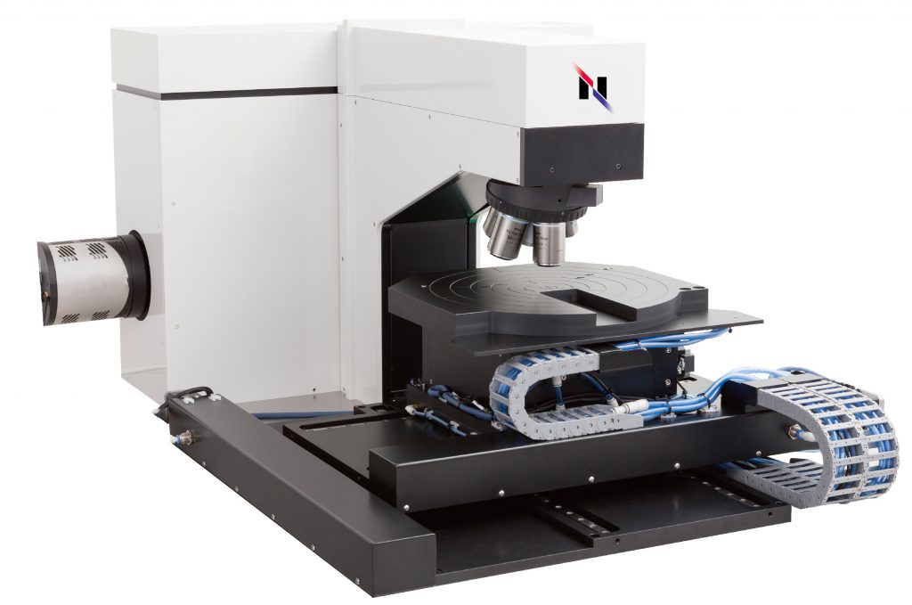
RAMANdrive presented in 2016.
In the previous interview, Ms. Adachi talked about the development of RAMANdrive, “We had a customer who wanted to analyze foreign substances by moving to specific coordinates on a large wafer, and we worked with them to commercialize the product. The RAMANdrive is equipped with a dedicated stage that can accommodate large wafers of up to 30 cm in diameter, and is capable of high-speed measurement of both the entire surface and small areas.
The development of RAMANdrive began in 2014 in response to customer feedback, and it was announced in August 2016. At that time, however, we had not yet envisioned “Raman imaging of the entire wafer,” so the AreaFlash function was not included.
Looking back on that time, Ms. Adachi said, “Now that we were able to measure large objects, we tried measuring the entire wafer, and it took more than a day. This was a sensation in the industry. Using line illumination technology that enabled high-speed measurement, we were able to obtain Raman images of the entire surface of a large wafer in a very short time, which was the norm at the time.
Reduce measurement time from over a day to 12 minutes
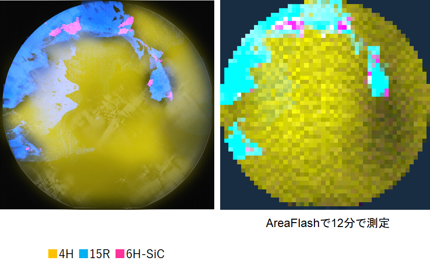
This was followed by the development of the AreaFlash function, which made it possible to measure wafers of the same size in as little as 12 minutes. The data below shows the difference in crystal structure of a 4-inch (10.16 cm) SiC (silicon carbide) wafer as observed by RAMANdrive. The Raman image on the left is a Raman image measured in detail using line illumination over a day, and the Raman image on the right is a Raman image measured using AreaFlash. although the resolution is lower with AreaFlash, it is possible to save a lot of time and effort by first measuring with AreaFlash and then measuring parts in detail as needed. The resolution is lower with AreaFlash.
The AreaFlash function was initially developed to obtain the average spectrum of a tablet.
AreaFlash was initially developed not for RAMANdrive, but for other uses.
”There was a request to use RAMANtouch to get the average spectrum of a drug tablet, and it was developed for use in the pharmaceutical field. We developed the RAMANtouch for use in the pharmaceutical field, because we wanted to get the average spectrum of a medicine pill. We used to do precise imaging, but now we can get the average Raman spectrum by shining the laser beam evenly over the entire field of view.
AreaFlash uses line illumination, which is also used in the Laser Raman Microscope RAMANtouch. Line illumination is a technique to simultaneously detect Raman scattered light from 400 points on the sample by stretching the laser beam in a line and irradiating the sample. AreaFlash swings this line illumination vertically at high speed to obtain the average spectrum of the laser beam over the entire field of view in a single exposure. It is very popular because it gives results in just a few seconds. “This is a feature only available with Nanophoton products that use Raman illumination. It is often used in the quality control department, where you can quickly find out how much of a certain impurity is contained,” says Adachi. Since the reaction process, such as the breaking of molecular bonds, can be measured in a short time, it is used not only in the pharmaceutical field, but also in various fields such as polymers and secondary batteries.
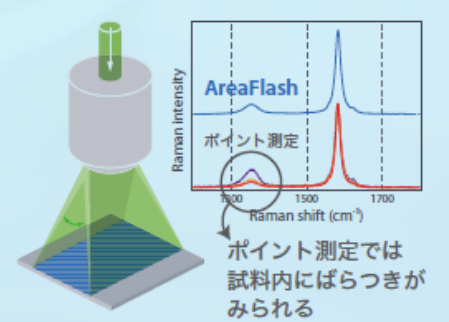
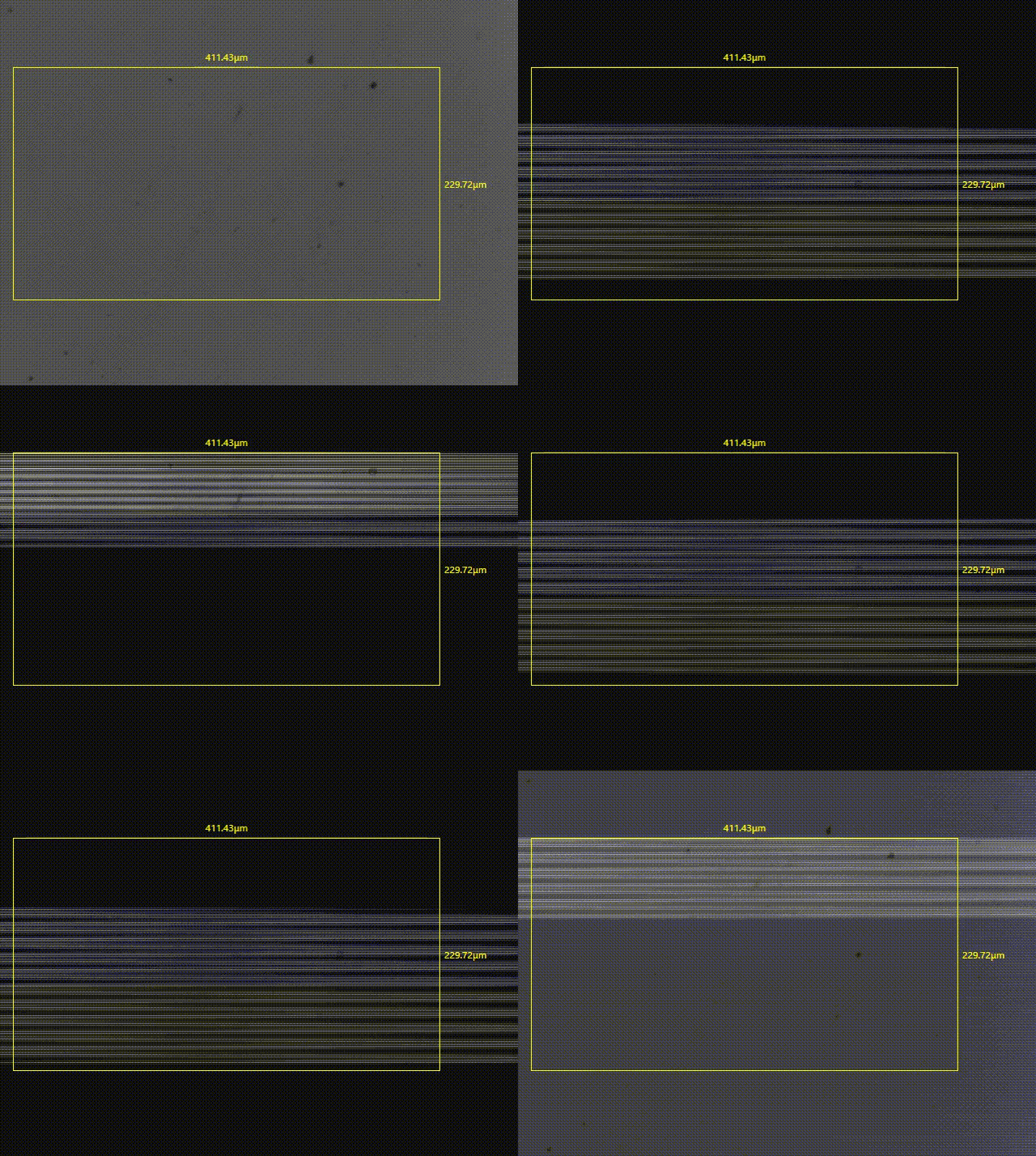
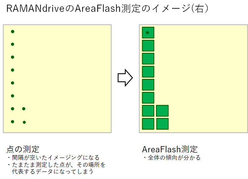
Ms. Adachi focused on the AreaFlash and thought that it could be used with the RAMANdrive to quickly measure large samples. “We decided to move the stage and measure the average spectrum one after another,” he said. We were able to reduce the time from more than a day to 12 minutes. This wide area measurement with the AreaFlash can also be done with the RAMANtouch if the sample size is up to about 15 cm.
It is also effective for stress measurement on the entire wafer surface.
AreaFlash measurement is also useful for measuring difficult stresses. In the figure below, the surface of a 30cm silicon wafer is scratched with a file and the stress caused by the scratch is measured. “With RAMANdrive, we can make measurements quickly, which we could not do before even if it took us many months,” says Adachi.

RAMANdrive’s stage navigation system
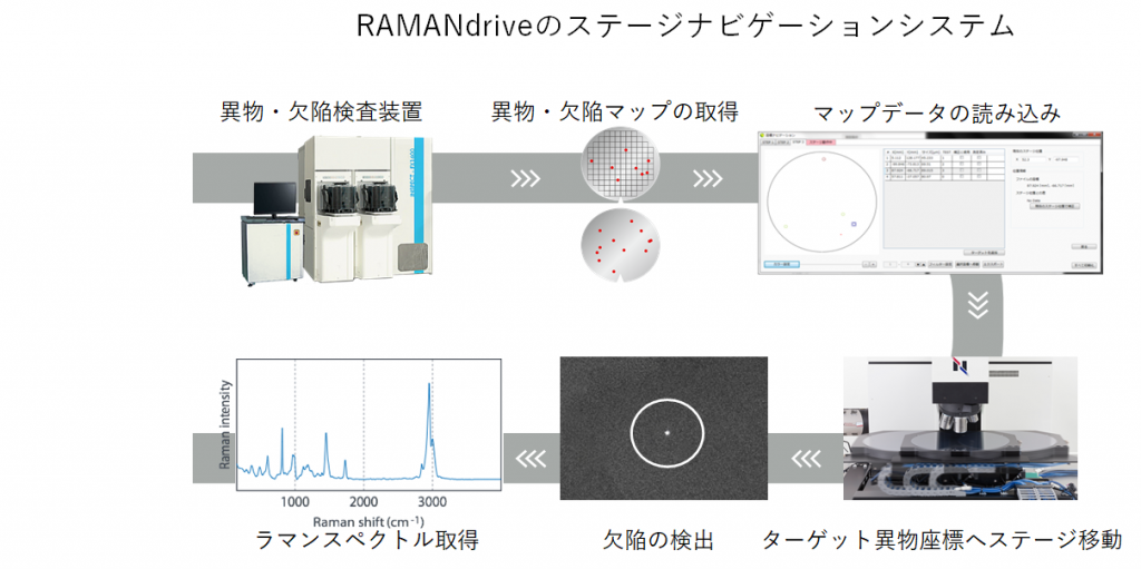
The “ability to move the stage and move to specific coordinates for measurement,” which led to the development of RAMANdrive, is called the stage navigation system.
“There is a surprisingly high level of news about the need to accurately move to a specific position for measurement, and the technology is being used in a variety of fields, not just wafers.”
Below is an image of the stage navigation system in use. When a foreign object or defect is found by the foreign object/defect inspection system, the coordinate information file is input into RAMANdrive, and the system immediately moves to that location to obtain a Raman image.
We will give you the latest catalog.
The functions and data introduced in this article are available in the latest catalog. If you would like to receive a copy, please fill out the inquiry form and send it to us in PDF format.
