Email Magazine
Report
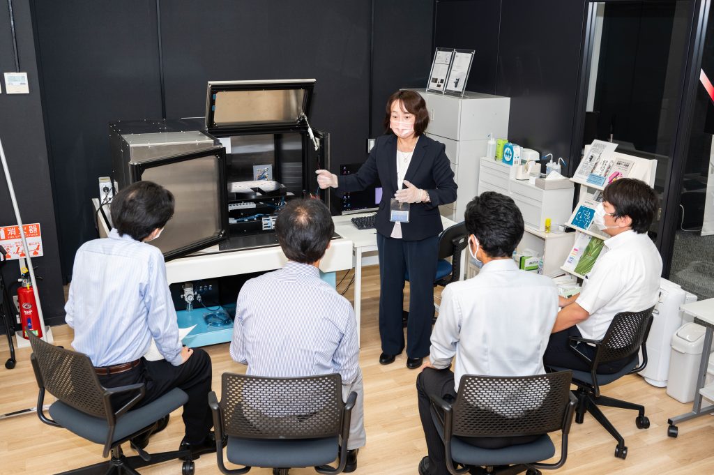
Nanophoton held its 1st Demonstration Seminar for FY2022 at its Osaka Showroom (Minoh, Osaka) on Friday, June 17. Due to COVID-19 pandemic, this is the first face-to-face meeting held at the newly established Osaka Showroom in three years since 2019. Representatives from four pharmaceutical and other companies were given the opportunity to see first-hand the performance and usage of four Raman microscopes. Participants listened intently to the explanations and asked many questions, which gave the Nanophoton employees in charge of the seminar a solid response. The demonstration seminar will be held again in the future. Here is a report on the seminar, which lasted about four hours. (Takeshi Nemoto, Editor-in-Chief of the Email newsletter/science writer)
“Work Reform with Ultra-fast Imaging!”
The theme of the seminar is “Work Reform with Ultrafast Imaging! Why Everyone Chooses Nanophoton.” . The lecture and demonstration were given by Mariko Adachi, Senior Engineer, Nanophoton Sales & Applications.
First, using a PowerPoint presentation, the lecture included an explanation of Nanophoton’s company and basic knowledge of laser Raman microscopy. We had to endure the lecture for a while.
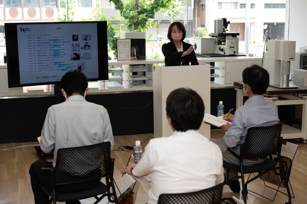
Furthermore, it is an explanation of Nanophoton’s product line and “what can be measured”. The explanation was easy to understand because it showed many measurement examples.
For example, she explained, “In a nutshell, laser Raman microscopy is ‘an optical microscope that allows you to see chemical images,'” and then showed a Raman image of an employee’s oral mucosa. Using the Raman microscope, proteins and lipids can be distinguished by differences in molecular structure and displayed in different colors on a computer screen. No pre-processing is required,” said Senior Engineer Adachi.
Other examples of measurements presented were
“Layer number distribution imaging of ultra-fast graphene”
“Raman spectra of yellowing of polyvinyl chloride exposed to sunlight”
“High resolution Raman imaging of lithium ion battery before and after charging”
“Imaging of crystallinity distribution around the threaded end of a plastic bottle”
“Surface stress imaging of silicon carbide substrate”
“Imaging evaluation of fiber orientation distribution in tea bags”
and many more. Through these measurement examples, we conveyed “what can be understood by Raman spectroscopic analysis”.
After that, the lecture ends with a detailed explanation of “5 things that Raman spectroscopic analysis can tell us,” “Why Nanophoton is chosen,” and “Points to choose a Raman microscope”. Finally, it is time for the demonstration.
<Five things Raman spectroscopic analysis can tell us>
1. Identification of substances (foreign material analysis, distribution analysis)
2. Change in molecular structure
3. Crystallinity
4. Stress
5. Orientation
<Why choose Nanophoton?>
1. Laser beam scanning – high operability
2. High spatial resolution
3. Ultra-fast imaging line illumination
4. High spectral performance, allowing measurement of small stresses
5. Highest detection sensitivity
6. Various measurement modes to meet various needs
7. Maintenance-free, highly stable system
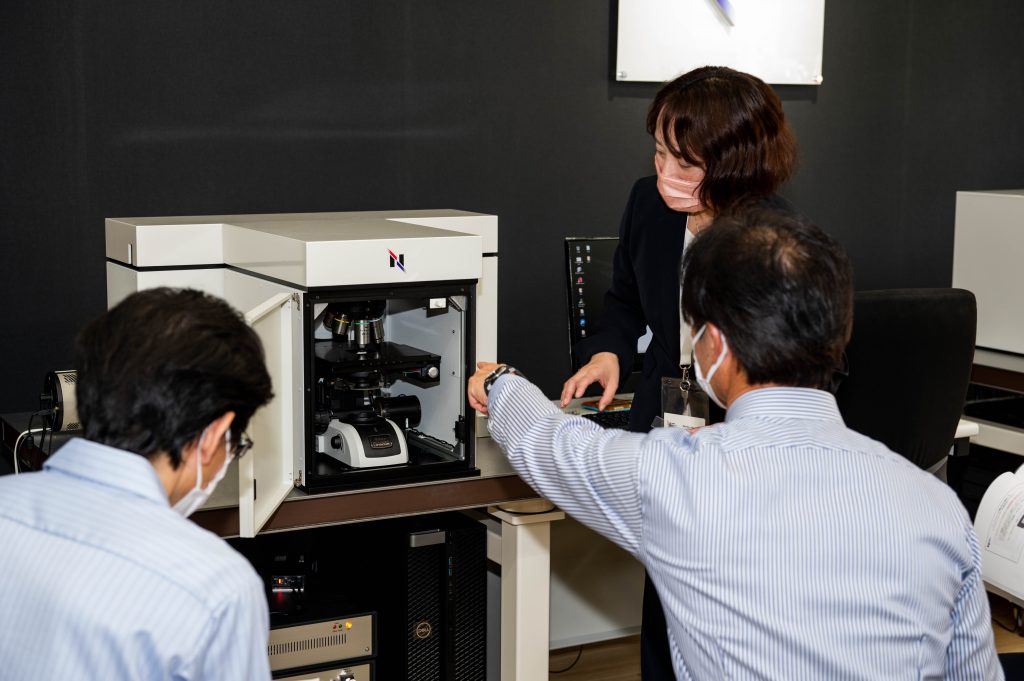
Demonstration with 4 models
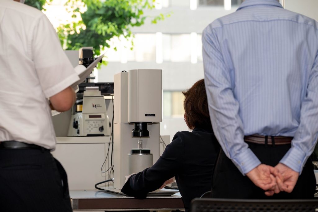
In the demonstration, various samples were measured using four models permanently installed in the Osaka showroom: RAMANwalk, a random scanning confocal Raman microscope; RAMANtouch, a laser Raman microscope; RAMANdrive, a Raman microscope with wafer stage; and RAMANview, a wide-field Raman scope.
First is RAMANwalk. By lowering the light-shielding cover, the stage can be accessed not only from the front but also from the left and right. We actually demonstrated surface imaging using the ZTrack function for samples with uneven surfaces, as well as the ability to change the laser wavelength for measurements with reduced fluorescence.
Next is RAMANtouch. The on-board “Line Illumination” function stretches the laser beam in a line to the sample and simultaneously detects Raman scattered light from 400 points to achieve high-speed measurement. We also had a chance to experience the convenience of the “area flash” function, which uses line illumination.
RAMANdrive can obtain Raman images of wafers up to 30 cm in length in a short time. In fact, a 30 cm wafer was set on the stage and the entire image was observed on the spot. Foreign object analysis using the coordinate navigation function was also demonstrated.
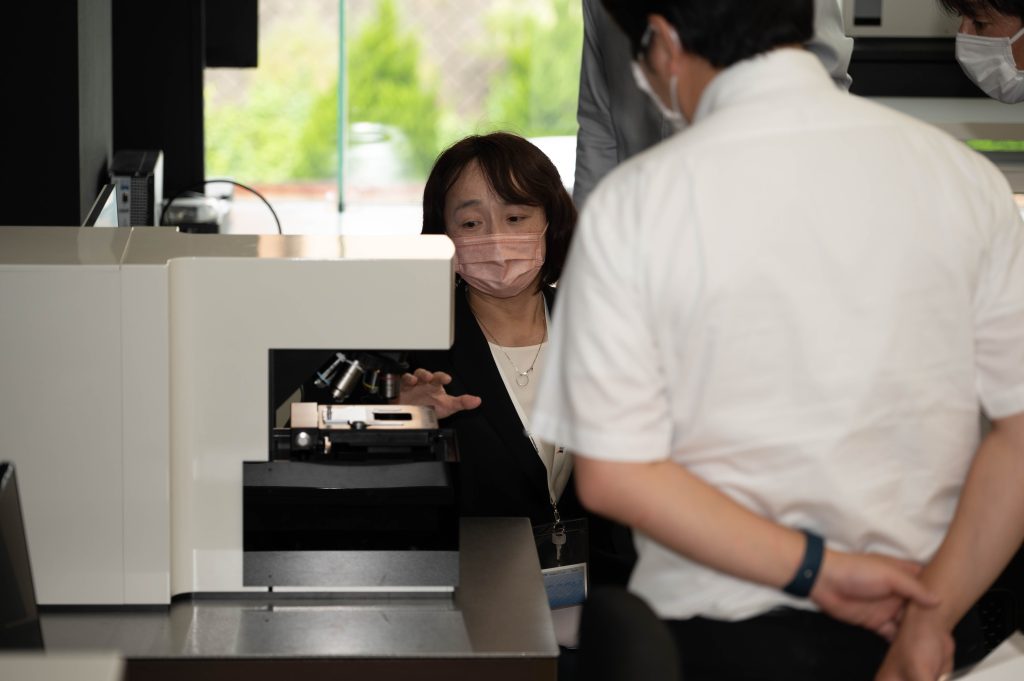
Finally, RAMANview allows for full-viewing of large samples, such as tablets, and is also good for measurements of samples with surface elevation differences.
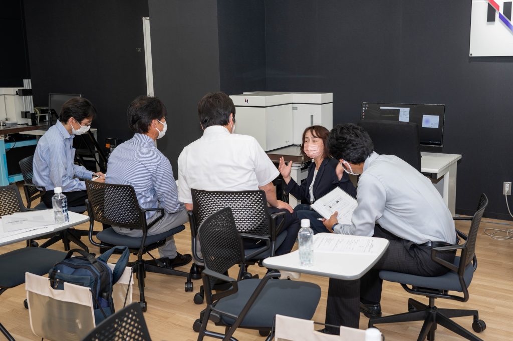
Demonstrations that were not in the program.
I felt that it was a very dense demonstration seminar. This was probably due to the fact that Nanophoton’s Raman microscopes are capable of making measurements at high speeds, so the waiting time is short. At the request of the participants, we also gave demonstrations that were not in the program, such as stress imaging and special objective lenses.
One of the participants said, “At my company, we use another company’s product that we purchased 13 years ago. This time, when I saw a demonstration, I was shocked at its performance, including clean mapping. I was satisfied with the seminar because it was a small group and I was able to freely ask questions about what I wanted to know.
To be held in the future
Demonstration seminars will be held in the future. Those interested in Raman microscopy of nanophotons are encouraged to attend.